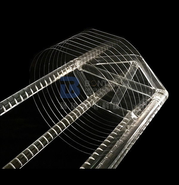
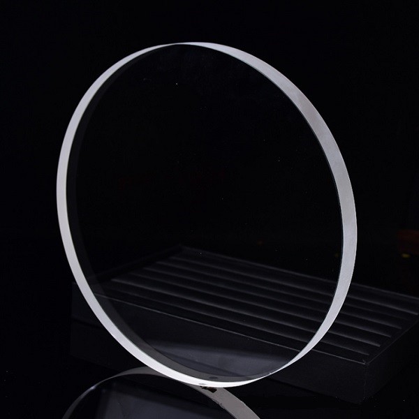
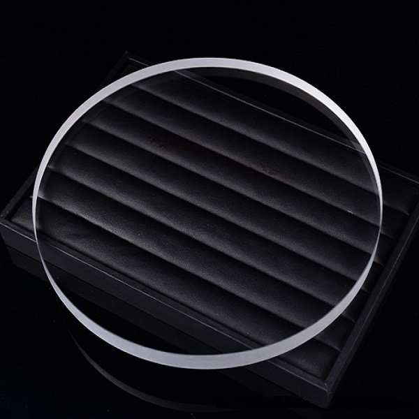
2" 3" 4" 6" 8" Fused Silica Wafer for High-Precision Semiconductor Manufacturing
our premium Wafer-Grade Fused Silica Wafers – the ultimate solution for your high-performance optical and microelectronic applications. Crafted from the purest fused silica, our wafers offer unparalleled optical clarity, thermal stability, and chemical resistance.
Designed for precision and durability, our Wafer-Grade Fused Silica Wafers are the perfect platform for creating cutting-edge optical components, waveguides, and micro-optical systems. Their low coefficient of thermal expansion ensures dimensional stability across a wide range of temperatures, making them ideal for use in demanding environments.
Experience superior transmission across the UV to IR spectrum, ensuring your optical systems perform at their peak. The high purity of our fused silica wafers minimizes scattering and absorption, delivering crisp, undistorted images and signals.
Whether you're developing advanced laser systems, fiber optic communication networks, or precision sensing technologies, our Wafer-Grade Fused Silica Wafers are the essential building blocks for success. Upgrade your optical and microelectronic designs with the unbeatable performance of our premium wafers – order now and elevate your projects to new heights!
| Parameter | Description |
| Material | Fused Quartz JGS2 |
| Composition | SiO<sub>2</sub> (Silicon Dioxide) |
| Transmission | Excellent transparency in the ultraviolet (UV) to infrared (IR) range |
| Refractive Index | 1.4585 (at 587.6 nm) |
| Density | 2.203 g/cm<sup>3</sup> |
| Thermal Expansion Coefficient | 5.5 x 10<sup>-7</sup> K<sup>-1</sup> |
| Operating Temperature Range | Up to 1,200°C |
| Chemical Resistance | Resistant to most acids, alkalis, and organic solvents |
| Surface Finish | Single or double-sided polished |
| Surface Quality | Typically specified as per industry standards (e.g., MIL-O-13830) |
| Dimensional Tolerance | Customizable as per customer requirements |
| Wafer Sizes | Available in various diameters: 2", 3", 4", 6", 8", and larger |
| Wafer Thickness | Typically ranges from a few millimeters to several millimeters |
| Applications | Optics, lasers, semiconductors, scientific instruments, etc. |
Fused Quartz Fabrication Specifications
| Parameter | JGS1 | JGS2 | JGS3 |
| Maximum Size | <Φ200mm | <Φ300mm | <Φ200mm |
| Transmission Range (Medium transmission ratio) | 0.17~2.10um (Tavg>90%) | 0.26~2.10um (Tavg>85%) | 0.185~3.50um (Tavg>85%) |
| OH- Content | 1200 ppm | 150 ppm | 5 ppm |
| Fluorescence (ex 254nm) | Virtually Free | Strong v-b | Strong V-B |
| Impurity Content | 5 ppm | 20-40 ppm | 40-50 ppm |
| Birefringence Constant | 2-4 nm/cm | 4-6 nm/cm | 4-10 nm/cm |
| Melting Method | Synthetic CVD | Oxy-hydrogen melting | Electrical melting |
| Applications | Laser substrate: Window, lens, prism, mirror... | Semiconductor and high temperature window | IR & UV
substrate |

FAQs:
- Q: What are the products you mainly work on?
A: We look at ourselves as the piezo wafer specialist. We are the very first to work with Single Crystal Quartz in China about 30 years ago. Then gradually we step in the field of LiNbO3, LiTaO3, Quartz glass, LGS, CTGS etc. Especially, if you are looking for a piezo quartz supplier, we are the ultimate choice! We export millions of quartz blanks each year because we master the AT, SC and IT cuts with superior angle precision.
- Q: Can you accept product customization?
A: Yes, of course. We can fabricate as per your request. In addition, we are so experienced with piezo wafers that we can provide you relevant suggestions if you are not 100% sure about your choice. Besides, we do have some standard wafers in stock, please check with us.
- Q: Can you deliver the goods via our courier agent?
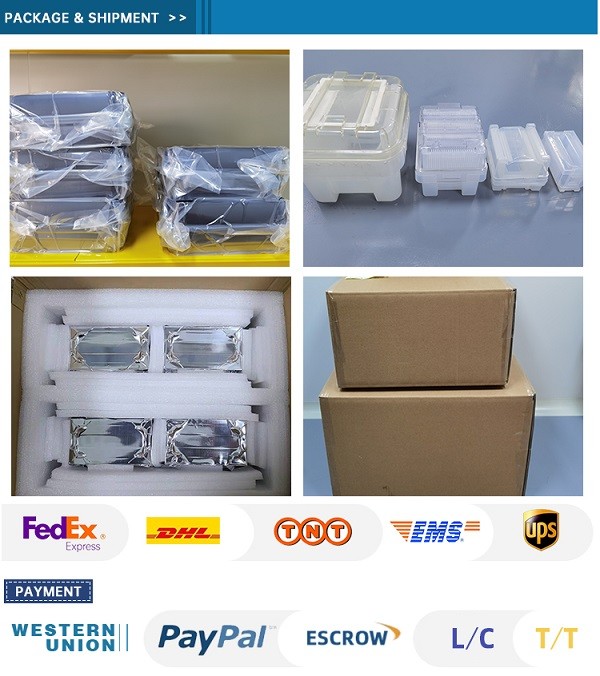
A: Yes, we would suggest you go with the courier agent you are most familiar with (DHL, FedEX, UPS etc.). We can ship via your account. And, of course, we will pack the products safely in acceptable size to help you save the shipping cost. If you need us to take care of the freight, it’s also not a problem. We also have good discount with the international courier companies.
- Q: How can you guarantee we get what we want safely?
A: The wafer products are fragile and sometimes expensive. The last thing, as the manufacturer, we want to see is the products we make were damaged during courier. As a result, we will pack the wafers adequately and put them in a proper carton filled with buffer sponge. However, accidents are inevitable sometimes. So, please follow the “Acceptance check” steps shown in the drawings below. If the unwanted happened, we will either give the replenishment or refund if you follow the checking steps.
- Q: Can we visit your factory?
A: Sure. Factory inspection is important for large quantity purchase and long-term cooperation. Face to face discussion is what we mostly confident with. During the past years, big names around the world have witnessed our progress in factory build-up. These days, due to the Covid-19 pandemic, we also had the experience of videoconferencing with global buyers.
Acceptance Check
- The product is fragile. We have adequately packed it and labeled it fragile. We deliver through excellent domestic and international express companies to ensure transportation quality.
- After receiving the goods, please handle with care and check whether the outer carton is in good condition. Carefully open the outer carton and check whether the packing boxes are in alignment. Take a picture before you take them out.
- Please open the vacuum package in a clean room when the products are to be applied.
- If the products are found damaged during courier, please take a picture or record a video immediately. DO NOT take the damaged products out of the packaging box! Contact us immediately and we will solve the problem well.
Product Tags:

|
|
2" 3" 4" 6" 8" Fused Silica Wafer for High-Precision Semiconductor Manufacturing Images
|