Product Description:
This Quartz Wafer is available in various sizes, with Primary Flat dimensions of 22mm, 32.5mm, 42.5mm, 57.5mm/notch, notch, notch. The wafer also has excellent PLTV (<0.5um) with a minimum of 95% in a 5mm x 5mm area. The TTV of the wafer is also impressive, with options of <8µm, <10µm, <15µm, <20µm, <30µm, and <30µm, catering to different needs and requirements.
One of the main advantages of this Quartz Wafer is its surface quality, which comes in three options - DSP, SSP, DSL. DSP or double-sided polished surface is smooth and flat, with both sides polished to a high level of precision. SSP or single-sided polished surface has one side polished, while the other side is rougher and is suitable for bonding applications. DSL or double-sided lapped surface is flat and smooth, but with a lower level of precision than DSP.
The JGS1 JGS2 JGS3 Glass and Quartz wafer for Superior Optical Clarity Chemical Stability is suitable for various applications, including but not limited to, MEMS, semiconductors, and microelectronics. It is widely used in the fabrication of microelectronic devices, optical components, and sensors, as well as in research and development.
Overall, the JGS1 JGS2 JGS3 Glass and Quartz wafer for Superior Optical Clarity Chemical Stability is a must-have for anyone looking for a high-quality Quartz Wafer that offers excellent optical and mechanical properties, precision, and clarity. Its availability in different sizes, surface quality, and TTV options make it a versatile option for various applications.
Features:
- Product Name: Fused Silica Wafer
- Edge Rounding: Compliant with SEMI M1.2 Standard/refer to IEC62276
- Product Category: Fused Silica Wafer
- Primary Flat: 22mm, 32.5mm, 42.5mm, 57.5mm/notch, notch, notch
- PLTV(<0.5um): ≥95%(5mm*5mm)
- Material: UV Fused Silica, Fused Quartz (JGS1, JGS2, JGS3)
Keywords: Silica Crystal Wafer, Fused Quartz Wafer, Amorphous Silica Wafer
Technical Parameters:
| Brand | Diameter | TTV | Polished side Ra | Warp | Application | Transmission | Surface | Bow | PLTV(<0.5um) |
| JGS1 | 50.8mm,76.2mm, 100mm, 150mm, 200mm | <8µm, <10µm, <15µm, <20µm, <30µm, <30µm | <1.0nm or specific per requested | <30µm, <40µm, <50µm, <50µm, <60µm, <60µm | Semiconductor, MEMS | Ultraviolet And Visible | DSP, SSP, DSL | ±20µm, ±25µm, ±40µm, ±40µm, ±60µm, ±60µm | ≥95%(5mm*5mm) |
| JGS2 | 50.8mm,76.2mm, 100mm, 150mm, 200mm | <8µm, <10µm, <15µm, <20µm, <30µm, <30µm | <1.0nm or specific per requested | <30µm, <40µm, <50µm, <50µm, <60µm, <60µm | Semiconductor, MEMS | Ultraviolet And Visible | DSP, SSP, DSL | ±20µm, ±25µm, ±40µm, ±40µm, ±60µm, ±60µm | ≥95%(5mm*5mm) |
| JGS3 | 50.8mm,76.2mm, 100mm, 150mm, 200mm | <8µm, <10µm, <15µm, <20µm, <30µm, <30µm | <1.0nm or specific per requested | <30µm, <40µm, <50µm, <50µm, <60µm, <60µm | Semiconductor, MEMS | Ultraviolet And Visible | DSP, SSP, DSL | ±20µm, ±25µm, ±40µm, ±40µm, ±60µm, ±60µm | ≥95%(5mm*5mm) |
Technical parameters for Silica Glass Wafer, Vitreous Silica Wafer, Crystalline Silica Wafer are shown in the above table.
Applications:
BonTek, a leading manufacturer of high-quality Fused Silica Wafer, introduces its top-of-the-line product that is perfect for various applications in different industries. Our Fused Silica Wafer is made from high-purity silica glass, which is an amorphous form of SiO2, making it highly resistant to thermal shock and chemical corrosion. It is available in different sizes and types, including Fused Silica and Fused Quartz, with a diameter of 50.8mm, 76.2mm, 100mm, 150mm, and 200mm.
BonTek's Fused Silica Wafer is certified with ISO:9001 and ISO:14001, ensuring that it adheres to international standards for quality and environmental management. It is manufactured in China, with a minimum order quantity of 5 pcs. The price is negotiable, and payment terms are T/T. We have a supply ability of 20,000 pcs per month, with a delivery time of 1-4 weeks, depending on your location.
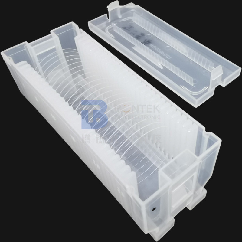
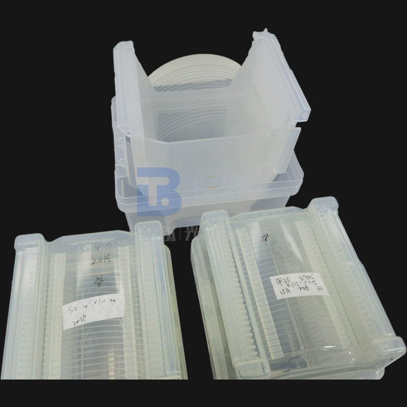
Our Fused Silica Wafer is vacuum-sealed, and we offer different packaging options, including cassette and jar packages. The PLTV of our product is ≥95% (5mm*5mm), making it highly reliable for your applications. The polished side Ra is <1.0nm or specific per requested, ensuring that the surface is smooth and defect-free.
BonTek's Fused Silica Wafer is ideal for various occasions and scenarios, such as in the semiconductor industry for microchip production, optical industry for lens and mirror fabrication, and solar industry for solar cell production. It can also be used in research and development for various fields, including physics, chemistry, and material science.
Investing in our Fused Silica Wafer will give you a competitive edge in your industry. Contact us today to place your order and experience the quality and reliability of our product!
Support and Services:
Our Fused Silica Wafer product is supported by our team of technical experts who are available to answer any questions or concerns you may have about the product. We offer a range of technical support and services to ensure that you get the most out of your Fused Silica Wafers. Our services include:
- Custom wafer specifications to meet your unique requirements
- Wafer polishing and cleaning services for optimal performance
- Wafer bonding and integration services for complex device structures
- Expert consultation on wafer design and fabrication
- Training and education on Fused Silica Wafer handling, storage, and usage
Our goal is to help you maximize the performance and reliability of your devices through our Fused Silica Wafer product and technical support services.
Packing and Shipping:
Product Packaging:
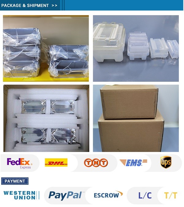
The Fused Silica Wafer product will be packaged securely to ensure safe delivery. Each wafer will be individually wrapped in anti-static material and then placed in a foam-lined box. The box will be labeled with the product name, quantity, and any other relevant information.
Shipping:
The Fused Silica Wafer product will be shipped via a reputable carrier such as FedEx or UPS. The shipping cost will be calculated based on the weight and destination of the package. We offer both domestic and international shipping options. Customers can choose from standard or expedited shipping depending on their needs and preferences.
FAQ:
-
What is the brand name of the fused silica wafer?
Answer: The brand name of the fused silica wafer is BonTek.
-
What are the models available for the fused silica wafer?
Answer: The available models for the fused silica wafer are Fused Silica and Fused Quartz.
-
What certifications does the fused silica wafer have?
Answer: The fused silica wafer has ISO:9001 and ISO:14001 certifications.
-
What is the minimum order quantity for the fused silica wafer?
Answer: The minimum order quantity for the fused silica wafer is 5 pcs.
-
What is the packaging details of the fused silica wafer?
Answer: The packaging details of the fused silica wafer are Cassette/ Jar package, vaccum sealed.
Note: For price, payment terms, supply ability and delivery time, please contact our customer support.