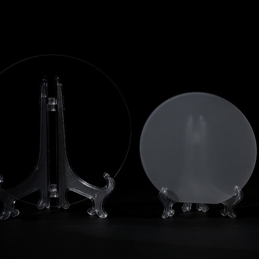
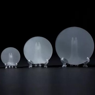
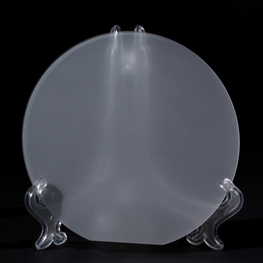
High Resistance Sapphire Polished Wafer 3 Inch C-Plane Optical Crystal
Sapphire is a single crystal of alumina and is the second-hardest material in nature, after diamond. Sapphire has good light transmittance, high strength, collision resistance, wear resistance, corrosion resistance and high temperature and high pressure resistance, biocompatibility, is an ideal substrate material for the production of semiconductor optoelectronic devices, the electrical properties of sapphire make it become the substrate material for the production of white and blue LED.
| Item | 3-inch C-plane(0001) 500μm Sapphire Wafers |
| Crystal Materials | 99,999%, High Purity, Monocrystalline Al2O3 |
| Grade | Prime, Epi-Ready |
| Surface Orientation | C-plane(0001) |
| C-plane off-angle toward M-axis 0.2 +/- 0.1° |
| Diameter | 76.2 mm +/- 0.1 mm |
| Thickness | 500 μm +/- 25 μm |
| Primary Flat Orientation | A-plane(11-20) +/- 0.2° |
| Primary Flat Length | 22.0 mm +/- 1.0 mm |
| Single Side Polished | Front Surface | Epi-polished, Ra < 0.2 nm (by AFM) |
| (SSP) | Back Surface | Fine ground, Ra = 0.8 μm to 1.2 μm |
| Double Side Polished | Front Surface | Epi-polished, Ra < 0.2 nm (by AFM) |
| (DSP) | Back Surface | Epi-polished, Ra < 0.2 nm (by AFM) |
| TTV | < 15 μm |
| BOW | < 15 μm |
| WARP | < 15 μm |
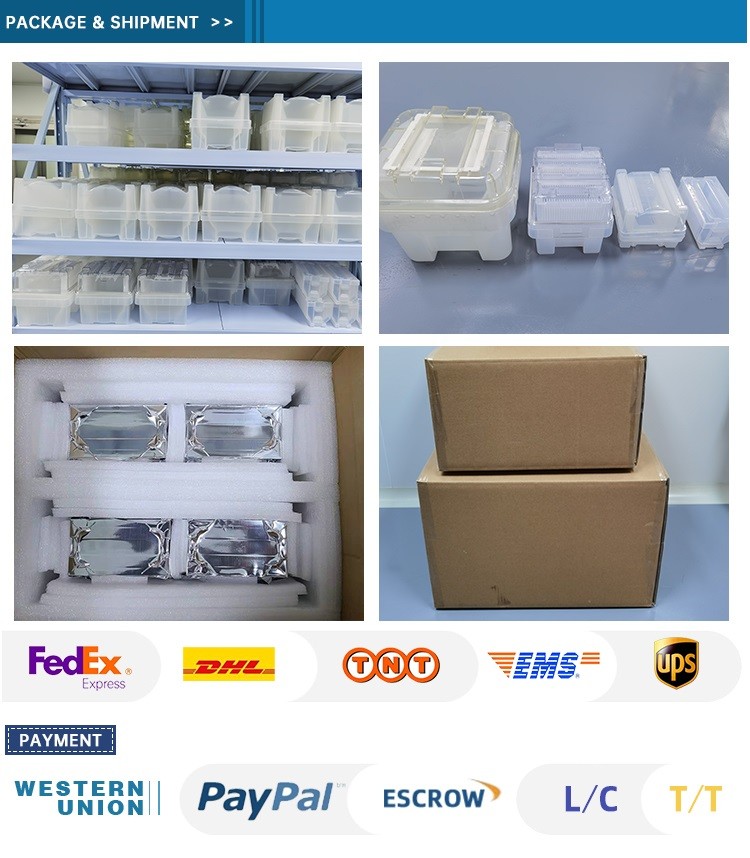
| Cleaning / Packaging | Class 100 cleanroom cleaning and vacuum packaging, |
| 25 pieces in one cassette packaging or single piece packaging. |
| Item | 4-inch C-plane(0001) 650μm Sapphire Wafers |
| Crystal Materials | 99,999%, High Purity, Monocrystalline Al2O3 |
| Grade | Prime, Epi-Ready |
| Surface Orientation | C-plane(0001) |
| C-plane off-angle toward M-axis 0.2 +/- 0.1° |
| Diameter | 100.0 mm +/- 0.1 mm |
| Thickness | 650 μm +/- 25 μm |
| Primary Flat Orientation | A-plane(11-20) +/- 0.2° |
| Primary Flat Length | 30.0 mm +/- 1.0 mm |
| Single Side Polished | Front Surface | Epi-polished, Ra < 0.2 nm (by AFM) |
| (SSP) | Back Surface | Fine ground, Ra = 0.8 μm to 1.2 μm |
| Double Side Polished | Front Surface | Epi-polished, Ra < 0.2 nm (by AFM) |
| (DSP) | Back Surface | Epi-polished, Ra < 0.2 nm (by AFM) |
| TTV | < 20 μm |
| BOW | < 20 μm |
| WARP | < 20 μm |
| Cleaning / Packaging | Class 100 cleanroom cleaning and vacuum packaging, |
| 25 pieces in one cassette packaging or single piece packaging. |
| Item | 6-inch C-plane(0001) 1300μm Sapphire Wafers |
| Crystal Materials | 99,999%, High Purity, Monocrystalline Al2O3 |
| Grade | Prime, Epi-Ready |
| Surface Orientation | C-plane(0001) |
| C-plane off-angle toward M-axis 0.2 +/- 0.1° |
| Diameter | 150.0 mm +/- 0.2 mm |
| Thickness | 1300 μm +/- 25 μm |
| Primary Flat Orientation | A-plane(11-20) +/- 0.2° |
| Primary Flat Length | 47.0 mm +/- 1.0 mm |
| Single Side Polished | Front Surface | Epi-polished, Ra < 0.2 nm (by AFM) |
| (SSP) | Back Surface | Fine ground, Ra = 0.8 μm to 1.2 μm |
| Double Side Polished | Front Surface | Epi-polished, Ra < 0.2 nm (by AFM) |
| (DSP) | Back Surface | Epi-polished, Ra < 0.2 nm (by AFM) |
| TTV | < 25 μm |
| BOW | < 25 μm |
| WARP | < 25 μm |
| Cleaning / Packaging | Class 100 cleanroom cleaning and vacuum packaging, |
| 25 pieces in one cassette packaging or single piece packaging. |
Acceptance Check

1. The product is fragile. We have adequately packed it and labeled it fragile. We deliver through excellent domestic and international express companies to ensure transportation quality.
2. After receiving the goods, please handle with care and check whether the outer carton is in good condition. Carefully open the outer carton and check whether the packing boxes are in alignment. Take a picture before you take them out.
3. Please open the vacuum package in a clean room when the products are to be applied.
4. If the products are found damaged during courier, please take a picture or record a video immediately. DO NOT take the damaged products out of the packaging box! Contact us immediately and we will solve the problem well.
Product Tags:

|
|
High Resistance Sapphire Polished Wafer 3 Inch C Plane Optical Crystal Images
|